IMSAI MPU-B

The IMSAI MPU-B is an 8085A processor board with a serial port, bi-directional parallel port, 3 timers, 256 bytes of RAM, and a 2K monitor ROM.
The 8085A runs at 3 MHz while maintaining similar bus timing of a 2 MHz 8080A due to the improved bus utilization of the 8085A.
These onboard peripherals make it possible to build a system without a front panel and an I/O interface card.
A RAM and disk controller card are all that is necessary to build a usable system.
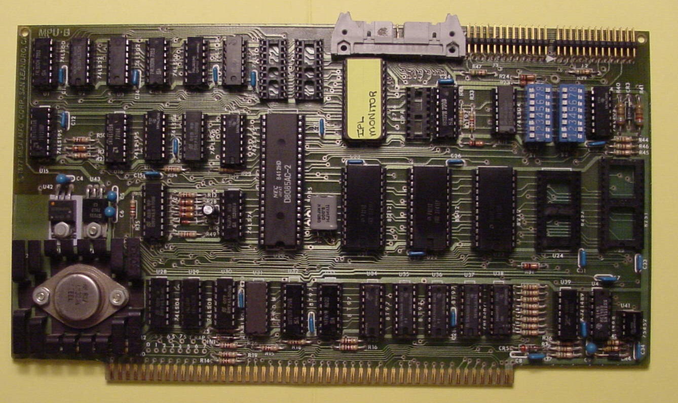
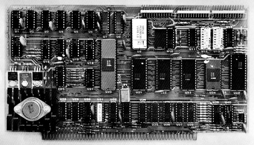
There are two MPU-B revisions in circulation, Rev 1.2 and Rev 2.
The easiest way to distinguish them is Rev 1.2 (pictured below) has three TO-220 regulators above the TO-3 regulator in the large
heat sink, and is designed for a three-supply EPROM such as the 2708 for the firmware.
You are more likely to encounter a Rev 2 MPU-B (pictured above) which has a single-supply 2716 for the firmware.
In later builds, a 8316 mask ROM was used which decreased cost and increased reliability (mask ROMs will not fade over decades like EPROMs can).
The MPU-B manual has some assembly errata. While this modification should be done on Rev 1.2 boards, the schematic has the corrections.
The errata itself has an error in the diagram. It shows U18 as U15.
- Contents
Visit our Facebook group for announcements, discussions,
and more information about supporting the IMSAI MPU-B.
We put a lot of time into creating, gathering, and organizing the information in this page.
If you found any of this to be useful to you, especially if it helped you to make or save money,
please
to help us continue making content like this available.
If you are moving an MPU-B into a new system, you should take the time to make sure it is set up properly based on your system’s hardware and software.
Address Map
The MPU-B drives the low 16 address lines and is unaware of the upper 8. Same for decoding.
The MPU-B has several onboard peripherals that may be switched in and out of memory space through an I/O control port.
The address ranges that may be occupied by the MPU-B are 2K at 0000 or 4K at D000. The control I/O port is at F3.
There is a bipolar PROM at U31 that decodes the memory and I/O addresses, which may be swapped out with one with different programming if you want to move things around.
If you move any of the addresses, you will need to write new firmware as the stock one expects to run at D800.
Jumper Areas
The MPU-B has several jumper areas on the board that must be properly configured.
P18, P19, and P21
If you have a Rev 1.2 board, make sure the jumpers are correct for the type of PROM in U9.
Consult the User Guide in the IMSAI MPU-B Reference Manual for details.
These jumpers are not present on Rev 2 boards.
MWRITE (68)
The MPU-B normally generates the MWRITE signal on J1-68.
There is a jumper area with 3 pads between U31 and U32 labeled WR, GND, and 68.
By default, a trace on the solder side connects pads RW and 68 to enable the WR signal to J1-68.
If you have an IMSAI CP-A or other card in the system that generates MWRITE, cut the trace on the solder side connecting pads RW and 68.
If you do not want to have an MWRITE signal on the bus, connect jumper pad GND to 68.
If you simply want to disable the MWRITE signal on the bus, you may set DIP switch 1-3 to OFF and skip the jumper cutting.
Interrupt Jumpers
The large jumper area near the left side of the S-100 connector allows you to assign any of the eight S-100 vectored interrupts
to one of the four new 8085 interrupt lines, RST 5.5, RST 6.5, RST 7.5 and TRAP.
It is important to note that by default, the MPU-B connects interrupt 6 to TRAP and interrupt 7 to the main PINT* line.
Make sure this is what you want, especially if you have another card with an interrupt controller.
DIP Switches
There are two DIP switches on the MPU-B. The reference manual is exceedingly confusing, so we have documented them here.
Hopefully our descriptions are more clear.
| Switch |
Label |
Description |
S1-8
S1-7 |
SPP
SPS |
SYSTEM PORT ENABLE. Only one of this pair of switches should be ON at a time. They cause either the serial or parallel I/O port (or neither) to respond to the system port addresses (02 data, 03 status). If switch 8 is ON, the parallel port is enabled. If switch 7 is ON, the serial port is enabled. If both switches are OFF, then ports 00 through 03 are unused, permitting an external I/O board (such as the MIO or SIO) to be installed using the bottom 4 ports. The MPU-B monitor requires a system port. |
S1-6
S1-5 |
CL |
CURRENT LOOP ENABLE. If current lop operation is desired, the CL switches should be ON. If synchronous mode is to be used, then the CL switches should be OFF. Switch 6 only present on Rev 2 boards. |
| S1-4 |
|
NOT USED. |
| S1-3 |
FPO |
FRONT PANEL INSTALLATION. This switch must OFF in any system with a CP-A installed. This is also the case with any other board which drives the S-100 MWRITE signal. Otherwise, this switch must be ON. |
S1-2
S1-1 |
T2C
T22 |
TIMER 2 CLOCK SOURCE. Only one of this pair of switches should be ON at a time. If switch 2 is ON, Timer 2 counts at a 2 MHz rate. If switch 1 is ON, Timer 2 increments one count at each high to low transition of the Timer 1 output. Cascading the timers this way and enabling only Timer 2 interrupts permits extended periods to be timed without software intervention. |
| S2-8 |
PII |
PARALLEL TRANSMIT READY INTERRUPT. If ON, a RST 6.5 interrupt will occur whenever the parallel I/O output buffer empty status is true (set by the handshake strobe). A jump to the interrupt service routine must be located at 0034. |
| S2-7 |
POI |
PARALLEL RECEIVE READY INTERRUPT. If ON, a RST 5.5 interrupt will occur whenever the parallel I/O input data ready status is true (set by the same strobe which latches data). A jump to the interrupt service routine must be located at 002C. |
| S2-6 |
SII |
SERIAL TRANSMIT READY INTERRUPT. If ON, a RST 6.5 interrupt will occur whenever the serial I/O transmit is enabled and the transmit buffer is empty. A jump to the interrupt service routine must be located at 0034. |
| S2-5 |
SOI |
SERIAL RECEIVE READY INTERRUPT. If ON, a RST 5.5 interrupt will occur whenever the serial I/O receive is enabled and a character is waiting to be input to the processor. A jump to the interrupt service routine must be located at 002C. |
S2-4
S2-3 |
T2I
T1I |
TIMER INTERRUPTS. Neither, either, or both of these may be ON a desired. Each switch will cause an RST 7.5 interrupt to occur when its respective timer output goes low. A jump to the interrupt service routing must be located at 003C. Timer 0 is the baud rate generator and is not connected to an interrupt. Note that RST 7.5 is an edge-triggered interrupt, so that timer modes which produce a terminal pulse may be used without danger of missing the interrupt. |
S2-2
S2-1 |
AS
S |
SERIAL RECEIVE CLOCK SELECT. Only one of this pair of switches should be ON at a time. If switch 2 is ON, the receive clock is the same as the transmit clock from the internal baud rate generator (Timer 0). This configuration is for asynchronous mode with a ×16 clock. If switch 1 is ON, the receive clock comes from pin 15 or pin 17 on the 25-pin serial connector depending if J2 or J3 is used. This configuration is for synchronous mode with a ×1 clock. |
The IEE-696 specification did not exist when the MPU-B was designed.
These modifications improve its compliance if you plan to use the MPU-B in a more compliant system.
These compliance modifications are presented in sections that may be implemented separately or in groups.
You probably do not want to do any of these modifications if the MPU-B is in a system with a CP-A front panel.
The CP-A is notoriously non-compliant and needs many of the signals these modifications delete.
Bus Signals
The IEEE 696 standard added, removed, and changed some previously-existing signals.
XRDY (3), NMI* (12)
The MPU-B does not use the XRDY bus signal on pin 3 (like the MPU-A does),
but it uses “XRDY2” (12) for the same purpose. Unfortunately, pin 12 is IEEE 696 NMI*.
This mod moves pin 12 to pin 3, and optionally hooks up NMI* to the 8085 TRAP input or something else appropriate.
No known IMSAI board uses pin 12. The CP-A drives pin 3 to “stop” the CPU in an indefinite wait state.
On the component side of the board, cut the trace from J1 (the S-100 connector) pin 12 at R14.
Leave some trace going to pin 12 for later. This releases pin 12.
Tack a “blue wire” from pin 3 to R14 which was cut loose in the previous step. This connects the circuit to the XRDY signal.
If you like, you may tack a jumper from pin 12 to one of the MPU-B’s interrupt pads if you want to use the bus NMI* signal.
The 8085A TRAP signal is a good bet. Hooking up NMI* is completely optional.
/DIDSBL (21)
J1-21 is no longer part of the IEEE 696 specification. If your system has a CP-A, do not remove this signal.
Otherwise, cut the trace between J1-21 and its nearest via. Deleting “unused” signals from the bus is completely optional.
pSTVAL* (25)
The Φ1 (pSTVAL*) signal is not disabled when a temporary master gets on the bus.
Do not do this mod if you have older DMA boards such as the IMSAI IFM, or if you do not have any IEEE 696-compliant TMA (DMA) boards in your system.
Open the reference schematic for this mod here.
Solder Side Cuts
- Cut the trace at U32-6.
- Cut the trace at U32-7.
Solder Side Adds
- Add a wire from U33-6 to U30-6.
- Add a wire from U33-7 to the via to J1-25.
PWAIT (27)
PWAIT is no longer part of the IEEE 696 specification. Many IMSAI boards use this signal (RAM 4A, RAM-16/32/65, RAM-III, VIO),
so removing it from the MPU-B should be done with careful consideration.
To remove it, cut the trace between J1-27 and its nearest via. Deleting “unused” signals from the bus is completely optional.
PINTE (28)
PINTE is no longer part of the IEEE 696 specification.
Only the IMSAI CP-A and PIC-8 board uses this signal, and the PIC-8 board does not work with the MPU-B anyway.
To remove PINTE, find the pad on the component side of the board near U33-16 labeled INTE.
Cut the trace between the INTE pad and R20.
RESET (75)
The MPU-A, MPU-B, and IFM all have an RC network on the signal line with a capacitor of several µF to ground.
This does not meet the IEEE 696 specification as open-collector, although it seems to function in most circumstances.
It is important that this signal is not terminated unless it is driven low at power-up by other means.
This is because the terminator resistors will greatly reduce the RC time constant of the reset circuit.
ERROR* (98)
SSTACK is now defined as an active-low bus error signal.
The default for the MPU-B is to connect this bus pin to GND, which will indicate a bus error.
This connection should be removed.
For Rev 1.2 boards, there is a jumper pad pair labeled STK on the component side near J1-50.
This jumper is installed as a trace on the solder side of the board. Cut that trace.
For Rev 2 boards, there is a jumper pad pair labeled STK on the component side near J1-50.
Unlike the Rev 1.2 boards, this jumper has been removed and replaced with a simple trace from J1-98 to GND.
On the solder side, cut the trace from J1-98 to GND.
Address Space
The MPU-B does not implement extended addressing. It drives A0 through A15 for a total memory address space of 65,536 bytes.
A bank-switch board such as the Parastream EAG-696 (on the drawing board) may be added to address the full 16,777,216 bytes.
We have a few upgrades here, all designed by Robert Weatherford. These modifications have been verified only on a Rev 2 board.
Please consider carefully the impact of any modification you do to your system before proceeding.
Consult the schematic and affected component datasheets and make sure you are comfortable with the suggested modifications.
Parastream Technologies does not assume responsibility for any impact these modifications will have on your system, good or bad.
Overclocking
Most of the upgrades here relate to “overclocking” the 8085.
Whether you are upgrading to a faster-spec 8085 (e.g. the 8085A-2 at 5 MHz), or running the clock into the 8085 past its limits,
there are some potential issues with the MPU-B itself you should consider before overclocking.
As you increase the system clock frequency, it puts more demand on the access times of several components in the MPU-B.
The good news is that all of these components are connected to the native 8085 bus, and the only additional delay is
through the low address latch (U21) which is 30ns maximum.
You can consult the 8085 datasheet and pretty accurately calculate the required access time.
The affected components are the 8085 itself (U20), RAM (U7, and U8), Firmware ROM (U9), 8253 (U24), and 8251 (U25).
Aside from the access time issues, the 8085 and 8253 also have clock frequency limits.
Not to say you can’t violate these, but you still want to have some operating margin — especially thermally.
Before overclocking, make sure your backplane is properly terminated and able to handle the higher frequency signals.
The early IMSAI backplanes such as the EXP-4, EXP-6, and EXP-22 are not up to the task.
S-100 Clock (Pin 49)
You may think that all you have to do is change Y1 to a higher frequency and you’re in overclock heaven. Not so fast.
The MPU-B generates the 2 MHz clock (on S-100 pin 49) by cleverly dividing the Φ2 clock by 1½. This works great if Φ2 is 3 MHz.
If you don’t have a reasonably accurate clock, the MPU-B serial ports (among other boards in the system) will not function properly.
This upgrade installs a dedicated 2 MHz crystal oscillator to free you to run your overclocking experiments without dealing with the
side-issues of an inaccurate pin-49 clock.
You have two installation choices. You can do the quick and dirty “dead-bug” installation with minimal fuss, or you can remove the
74LS109 from U26 and install it there. Each method has pros and cons.
Open the reference schematic for this upgrade here.
Installation at U26
 Removing the 74LS109 currently in U26, cutting a couple of traces, and installing the oscillator is the best-looking way to go,
but you are cutting a couple of traces on the board.
If you absolutely hate that idea, you may want to consider the dead-bug installation method.
Look at the photo to the right to see what the upgrade looks like on our socketed reference board.
Removing the 74LS109 currently in U26, cutting a couple of traces, and installing the oscillator is the best-looking way to go,
but you are cutting a couple of traces on the board.
If you absolutely hate that idea, you may want to consider the dead-bug installation method.
Look at the photo to the right to see what the upgrade looks like on our socketed reference board.
Component Deletions
- Remove U26. If you’re lucky and it’s in a socket, this is pretty easy.
Otherwise, be careful to preserve the board, not the chip. Cut out the chip and the clean out the holes.
Component Changes
- Install the 2 MHz oscillator as far away from the heat sink as it will go, with pin 1 direction consistent with the other ICs on the board.
You should end up with the oscillator pin 1 in U26-5 and pin 8 in U26-12.
Solder Side Cuts
- Cut the trace at U18-11.
- Cut the trace at U26-12.
Solder Side Adds
- Add a wire from U26-16 to U26-12.
- Add a wire from U26-9 to U32-4.
Dead-bug Installation
Mounting the oscillator upside down between U27 and U31 and wiring it into the board is a less-intrusive way to go.
You may choose between removing U26 or cutting one board trace. With the oscillator, you don’t need U26.
Removing it is just one less chip to consume power.
If you decide you want to restore the MPU-B to its original configuration later, just remove the oscillator and its wiring,
replace U26, and you’re back in business.
Component Additions
Using double-sided sticky tape, mount the oscillator module upside-down above U31, so its pin 1 is oriented to the right.
Solder Side Cuts
- If you are not removing U26, cut the trace at U18-11.
Wire Adds
The wires to be added will be first run through nearby vias and soldered to the designated oscillator pins.
The other end will be cut to length, stripped, and soldered to the designated IC pin on the solder side.
- Add a wire from the oscillator pin 4 to the ground via near U32 on the component side.
- Add a wire from the oscillator pin 8 to the +5V via near Y1 on the component side.
- Add a wire from the oscillator pin 5 to U32-4 through a via near U32 on the solder side.
Address Line Drive
 The lower 8 address lines are latched using an 8212 in U21.
The 8212 does not have good bus drive characteristics as it only sinks 15mA and sources -1mA — far less than the 24mA/2mA
requirements of IEEE 696. In addition, it is fabricated using the Schottky TTL process, which is not recommended for driving
transmission lines. In most stock applications, this seems to work fine, but if the backplane presents a high-current termination
load, the 8212 drive may be insufficient. The drive characteristics may become more problematic if you overclock the board.
The lower 8 address lines are latched using an 8212 in U21.
The 8212 does not have good bus drive characteristics as it only sinks 15mA and sources -1mA — far less than the 24mA/2mA
requirements of IEEE 696. In addition, it is fabricated using the Schottky TTL process, which is not recommended for driving
transmission lines. In most stock applications, this seems to work fine, but if the backplane presents a high-current termination
load, the 8212 drive may be insufficient. The drive characteristics may become more problematic if you overclock the board.
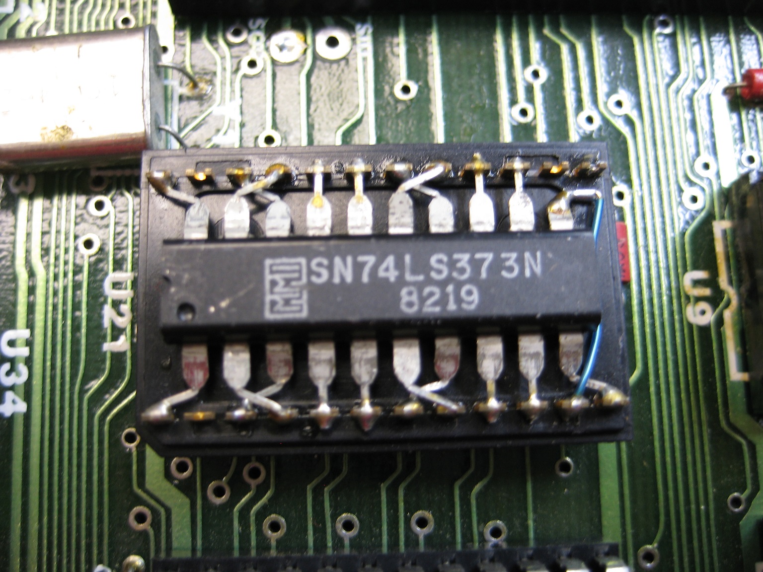
One proven way to fix the drive issue is to replace the 8212 with a latch and bus transceiver such as the 74LS373.
The photo to the right shows our reference MPU-B with a 24-pin socket header with a 74LS373 tortuously soldered into it to
match the 8212 pinout.
You may duplicate what is shown in the photo, or you may purchase a small, nice-looking circuit board from us that fits in the
U34 position (socketed or not). It uses the 74ALS373 for lower power at the same propagation delay.
A similar issue exists on the status signals. These are generated by a 74S288 PROM in U38.
The 74S288 has similar drive characteristics to the 8212 and makes a poor bus driver for all the same reasons.
Unfortunately, we do not have a fix ready for this. We are certainly going to try to.
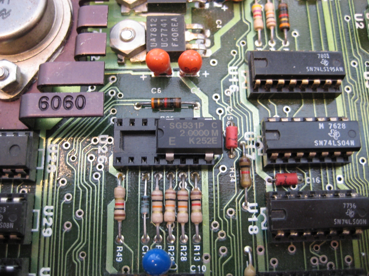
−12V Rail Stability
We have seen some problems with oscillation on the −12V rail because it does not have a bypass capacitor near the 7912 output terminal.
Install a 1µF 35V solid tantalum capacitor between the outer terminals of the 7912 with the + capacitor lead on the leftmost terminal
as you face the 7912 (viewed from the board top or hold the board upside-down).
Upgrade Parts
Some of the upgrades may require new parts. You can source them yourself, or save the hassle and pick them up here.
Replacement Parts
If your board needs replacement parts, you may find some of them here.
If you want parts that are from the time of manufacture, look here
for vintage replacements.
When the MPU-B starts up, its monitor firmware is present from address 0000 through 07FF and D800 through DFFF.
It then disables itself in the address range 0000 through 07FF and jumps to itself in the range D800 through DFFF.
At this point, the monitor is waiting for one of the following to happen:
- The IFM (if present) reads the boot sector from drive A. If this happens, the boot sector is executed and CP/M or IMDOS is booted.
- The DIO or MDIO reads the boot sector from drive A. If this happens, the boot sector is executed and CP/M or IMDOS is booted.
- A character is presented on the control port, MIO, or SIO ports 2 and 3 (see Control Port). The monitor is entered using the control port (see Monitor).
Monitor
The MPU-B monitor can use a VIO board at the default address of F800.
Parallel Port Operation
The monitor will work with the onboard parallel port. The most common use is with an IKB-1 keyboard and a VIO board.
Connect a 26-pin DB25 cable to J4 (the left header) and a IKB-1 or other parallel character entry device to the DB-25 connector.
DIP Switch SPS (left DIP switch 7) on the MPU-B must be OFF and SPP (left DIP switch 8) must be ON for the monitor to use the
onboard parallel port. The system waits for you to press the space bar to enter the monitor.
PARALLEL
IMSAI MPU-B MONITOR    VERS 1.3
?▒
Serial Port Operation
The monitor will work with a serial port. For the SIO, it must be addressed as ports 2 and 3, which is the default,
and the baud rate is fixed. DIP Switch SPS (left DIP switch 7) and SPP (left DIP switch 8) on the MPU-B must be OFF for the monitor to use the SIO.
The monitor can use the MPU-B onboard serial port. Connect a 26-pin DB25 cable to J3 (the center header) and a terminal or
other DTE equipment to the DB-25 connector.
Alternatively, you can connect the cable to J4 (the rightmost header) and a computer or other DCE equipment to the DB-25 connector
without having to use a "null modem." DIP Switch SPS (left DIP switch 7) on the MPU-B must be ON and SPP
(left DIP switch 8) must be OFF for the monitor to use the onboard serial port.
The system waits for you to press the space bar to enter the monitor, and automatically determines the baud rate:
300, 600, 1200, 2400, 4800, or 9600. The manual says it supports 110, but we could not get that to work.
9600 BAUD SERIAL
IMSAI MPU-B MONITOR    VERS 1.3
?▒
Commands
Refer to the IMSAI MPU-B Reference Manual for the monitor commands. Below is a preview showing how to display the first 256 bytes of the MPU-B firmware.
?D D800,D8FF

D800  3E 40 D3 F3 C3 10 D8 C3 3B DE C3 66 DE C3 EF D9  >@......;..f....
D810  31 E4 D0 21 80 00 22 FE D0 CD 7B D8 3D CA A7 D8  1..!.."...{.=...
D820  AF 32 F7 D0 21 FD FF 3E 56 BE C2 3C D8 23 3E 49  .2..!..>V..<.#>I
D830  BE C2 3C D8 3E 10 32 F7 D0 CD 00 F8 21 FA D0 22  ..<.>.2.....!.."
D840  F8 D0 3E AE D3 03 3E 27 D3 03 CD AE D8 21 A7 DF  ..>...>'.....!..
D850  CD 59 DE 31 E4 D0 21 56 D8 E5 CD B5 DE 3E 3F CD  .Y.1..!V.....>?.
D860  66 DE CD 3B DE 21 44 DF CD 8A DE CD E1 DD C8 CD  f..;.!D.........
D870  DB DE 06 01 E9 21 95 DF C3 68 D8 CD CA DC 21 F5  .....!...h....!.
D880  D0 3A FD E7 D6 44 C2 91 D8 3A FE E7 D6 49 CA 96  .:...D...:...I..
D890  D8 36 04 C3 EC DC CD 0C E0 36 02 CD EC DC F0 21  .6.......6.....!
D8A0  F5 D0 36 01 C3 EC DC 3E C0 D3 F3 C3 00 00 DB 14  ..6....>........
D8B0  21 C7 DF CD 59 DE 21 F7 D0 3E 10 A6 77 2B AF 77  !...Y.!..>..w+.w
D8C0  CD 53 D9 06 00 DB 12 B7 CA CC D8 04 CD 05 DE C2  .S..............
D8D0  20 D9 CD FD DD C2 31 D9 78 B7 CA CC D8 CD F5 DD   .....1.x.......
D8E0  CA CC D8 3C CA CC D8 06 00 CD F5 DD CA E9 D8 04  ...<............
D8F0  B7 CA E9 D8 21 1E DF 23 7E B7 CA B0 D8 B8 23 DA  ....!..#~.....#.

?▒
Control Port
The MPU-B manages its memory-mapped ROM, RAM, and Timers through the write-only port F3:
- Bit 6 (mask 40) controls whether the firmware ROM is mapped into the address space. Setting this bit to 0
(which is the default after a power-up or reset) maps the ROM to address 0000 through 07FF.
Setting this bit to 1 unmaps the ROM and allows the CPU to access system memory for address 0000 through 07FF.
- Bit 7 (mask 80) controls whether the firmware ROM, RAM, and the Timers are mapped into the address space.
Setting this bit to 0 (which is the default after a power-up or reset) maps the ROM to address D800 through DFFF,
the RAM to address D000 through D0FF, and the Timers to address D100 through D103.
Setting this bit to 1 unmaps the ROM, RAM, and Timers and allows the CPU to access system memory for address D000 through D103,
and address D800 through DFFF.
It is legal to map the ROM in both address ranges, one or the other, or not at all.
The status of the control port is available on port 15 bits 6 and 7.
The control port waits for 3 additional machine cycles before any changing the memory map to allow a JMP or CALL instruction to execute.
Interrupts must be disabled during this time as any INTA cycles would be counted. DMA cycles are not counted.
We put a lot of time into creating, gathering, and organizing the information in this page.
If you found any of this to be useful to you, especially if it helped you to make or save money,
please
to help us continue making content like this available.
Schematic
The schematics listed here were initially scanned by Herb Johnson.
You should check out his IMSAI collection at https://www.retrotechnology.com/herbs_stuff/d_imsai.html.
The corrections and markups for the upgrade mods were done by Robert Weatherford.
Manuals
Programmed Parts
If you want to program your own EPROMs and PROMs, here are the images:
IC Datasheets
|