IMSAI VIO

The IMSAI VIO is a memory-mapped 80×24 character display board.
It was originally introduced for the VDP-80 video data processor.
The term “personal computer” had yet to be coined.
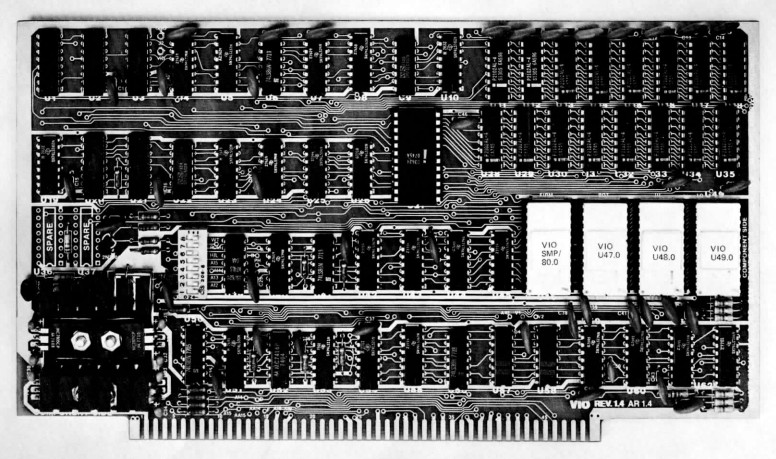
There are two VIO revisions in circulation, VIO-C and VIO-D. The VIO-C (pictured above) outputs composite video only.
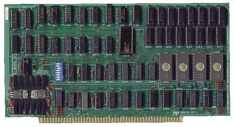
The VIO-D (pictured below) has a 7-pin connector at the top-left of the board that outputs TTL sync and composite video.
The VIO has 2 KB of firmware ROM and 2 KB of video RAM.
By default, this 4 KB block is positioned in the address space F000 through FFFF.
By adding a documented jumper, the 1 MB address space FF000 through FFFFF may be used.
Note to later IEEE 696 24-bit addressing systems.
The VIO does not decode the upper 4 bits of the address lines (A20 through A23),
and it can only decode lines A16 through A19 to enable the VIO at xFF000 through xFFFFF if you use the M jumper.
This will be an issue if you are using a CPU or other bus master that uses all 24 address lines.
We have some suggestions as to how to address this issue in IEEE 696 Compliance.
Perhaps the biggest challenge in using a VIO in the 21st century is the availability of video monitors.
The monitors IMSAI used were open-frame OEM units that were easily adjustable to dial in the video image.
The timing is close to NTSC (15.6 kHz and 60 Hz),
but some NTSC monitors have such a long vertical retrace interval that the top several lines of video are cut off.
We haven’t looked into the availability of monitors since the late 1980s.
We hope to create a page of monitors that you can buy now that can be easily made to work with the VIO.
Another option is to use a modern monitor (MDA, CGA, EGA, or VGA) and perform an appropriate upgrade.
Visit our Facebook group for announcements,
discussions, and more information about supporting the IMSAI VIO.
We put a lot of time into creating, gathering, and organizing the information in this page.
If you found any of this to be useful to you, especially if it helped you to make or save money,
please
to help us continue making content like this available.
Setup
If you are moving a VIO into a new system, you should take the time to make sure it is set up properly based on your system’s hardware and software.
Address Map
The VIO decodes up to 20 address bits, may be configured to occupy 2K or 4K of memory space in 4K increments starting at
x000, x800, Fx000, or Fx800. The VIO does not use any I/O ports.
Jumper Areas
The VIO has several jumper areas on the board that must be properly configured. Pay particular attention to jumper F.
Jumpers A, B
The A and B jumper pads are between U39 and U40 and is provided to optimize the address latch timing between the MPU-A and MPU-B.
Jumper A to PH for an 8080 CPU or B to PH for an 8085 CPU.
Because the VIO may be used with other processors, it is probably worth going into more technical detail as to what this jumper does.
Refer to the top-center of the IMSAI VIO Schematic where the pSYNC and Φ1 are NANDed.
Jumpering PH to A latches the state of the address lines on the rising edge of Φ1 which is 90ns after the address lines are stable
(not counting delays in the MPU-A and the VIO).
For the MPU-B, the Φ1 is actually the inverted Φ2 (8085 clock) signal.
The pSYNC signal is the 8085 ALE signal, and the addresses are not guaranteed to be stable until the clock rises
(the generated Φ1 falls). This means that you must latch the addresses on the falling edge of pSYNC • Φ1.
If you want to be strictly IEEE 696 compliant, jumper PH to B.
This will latch the address on the falling edge of pSTVAL* (which is Φ1 on the VIO schematic).
The address bus is not stable on the rising edge.
Even if you are running with an MPU-A, jumpering this way will only delay the address latching by 60ns.
Jumpers C and D
The C and D jumpers are relevant only if you have an IMSAI IMM running in your system.
As far as we know, no IMM boards were ever sold. If you do need to know, the VIO manual says to consult the IMM documentation.
If you have an IMM board, we would love to know about it!
Jumper F
The F jumper is located near S-100 bus pin 15 and is used to assert the PHANTOM* signal on the S-100 bus to disable system RAM
when the VIO is being addressed. If you have 64K or more of RAM in your system, you will need to do something with this jumper.
Otherwise, you will have both your RAM and the VIO driving the data in bus at the same time. On IMSAI systems,
A16 and A19 are typically used as a PHANTOM line, which is why those are the two jumper options.
For an IEEE 696 compliant system, pad F should be jumpered to A19, which is the IEEE 696 PHANTOM*, pin 67.
Jumper M
The M jumper is located between U53 and U54 on the board.
If your system is a 1 MB system (drives 20 address lines), you can use the M jumper to place the VIO in the top 64K page.
If your system is a 16 MB system (drives all 24 address lines), the M jumper will cause the VIO to appear in every 16th
64K page starting at page zero.
If you have other extended addressing requirements, we (will) have a small circuit board that may be added to a VIO to extend
the address decoding to a full 24 bits.
DIP Switches
Switches 1 through 4
Switches 1 through 4 set the base address. The default is all OFF, setting the base address to F000.
Switch 5
Switch 5 determines whether the VIOROM is in the upper 2K VIO address space.
If the switch is on, the VIOROM resides in the upper 2K and the VIO RAM is in the lower 2K;
otherwise, the VIOROM resides in the lower 2K and the VIO RAM resides in the upper 2K.
The default is OFF, placing the VIOROM at F800 and the VIO RAM at F000.
Switch 6
Switch 6 determines whether the VIOROM is active.
If the switch is ON, the VIOROM is active at the address range specified by switch 5;
otherwise, the VIOROM is disabled, and the VIO only occupies 2K in the system for the VIO RAM. The default in ON.
Switch 7
Switch 7 is used to enable a one-cycle wait state on all VIOROM and VIO RAM accesses.
Be advised that if your bus masters do not drive the legacy PWAIT signal (bus pin 27),
the wait state generator will not function.
Switch 8
Switch 8 is not used by the VIO. The No Snow upgrade uses it to enable the feature.
IEEE 696 Compliance
While the IEEE 696 bus was mostly backwards compatible with the S-100 bus of this era,
there were some significant changes that affected front panels and the like.
We try to address any potential IEEE 696 compatibility issues here.
Bus Signals
The IEEE 696 standard added, removed, and changed some previously-existing signals.
PWAIT (27)
The PWAIT signal on pin 27 was removed by the IEEE 696 standard, and is now RFU.
While all IMSAI CPU and IFM boards generate this signal, other CPU boards and bus masters may not.
If pin 27 is not driven, the VIO wait state generator will not function.
This may be a problem if the CPU board is too fast for the VIO refresh RAM.
Considering the way the VIO wait state generator is designed, there is no easy workaround.
Address Space
If the VIO is in a system that has a CPU board or other hardware that drives the extended address lines A16 through A23
to address more than 64 KB of memory, this section will be relevant to you.
We have some information and a few suggestions that might be helpful.
The Standard IMSAI solution
IMSAI was one of the first S-100 system suppliers to even think about RAM beyond 64 KB.
More on this at the end of this page for anyone interested in a bit of IMSAI history.
Starting with the RAM series (not including the RAM 4A), they extended the S-100 bus to 20-bit addressing to make way for the
IMM (Intelligent Memory Manager).
This included the RAM-16, RAM-32, RAM-65, RAM-III series, and the DIO, MPU-B,
and VIO which were memory-mapped.
In fact, 3 of the 4 IMSAI extended address lines made it into the IEEE 696 specification unchanged.
The standard IMSAI extended address for the VIO was FF000 through FFFFF (the upper 4 KB of the 1 MB address space).
As mentioned in the intro, the VIO does not decode the upper 4 bits of the address lines (A20 through A23),
and it can only decode lines A16 through A19 to enable the VIO at xFF000 through xFFFFF.
If this is what you want, add a wire between the two pads in the M jumper area.
If you want to be more IEEE 696 compatible, you will have to move the A19 line.
The A19 line is on J1-67 and should be on J1-59.
- On the component side of the board, cut the trace from the pad labeled A19. TODO: NO NOT DO THIS! A19 is PHANTOM* WHICH MANY USERS WILL NEED!
- On the solder side of the board, add a wire from J1-59 to U54-9.
20-Bit Addressing Solutions
If the VIO is in a system that uses only 20 of the 24 address lines (e.g. a 1 MB system), you can use
The Standard IMSAI solution described earlier if you want the VIO in the memory space FF000 through FFFFF.
Otherwise, you will need to come up with a different solution.
The VIO-C has two spare 16-pin IC positions to help, but the VIO-D only has one,
and if you have done the 25-Line Display or 25-Line Display HD
upgrades, you have no spare positions. This is made worse because there are no spare gates at all on the VIO.
If you do have a spare IC position, you could add a 74LS04 to invert some of the address lines as necessary going to U54 and
user the M jumper. Even if you do not have a spare position, you could add the inverter on top of U54 (a process we used to
call “dead-bugging”).
24-Bit Addressing Solutions
If the VIO is in a system that uses all 24 address lines (e.g. a 16 MB system), your options are a bit more limited.
Now, you need to decode at least 4 additional address lines.
Depending on the address you want to decode, you might wind up having to decode all 8.
A solution commonly used at IMSAI is to use an address decoder BPROM.
A 256×4 or 512×4 PROM would do the trick, if you can find and program one.
Another idea is a GAL, but now you’re looking at a 20-pin device in a 16-pin position.
If you come up with an elegant solution, we’d like to hear about it!
Phantom Addressing
TODO: this is probably not worthy of calling it an upgrade; just a way to use the Phantom* line to enable the board.
TODO: NOT SO FAST! I now remember why I did that seemingly stupid mod to keep the VIO off the data bus.
It was a quick and dirty way to deal with the RAM-III conflicting with it.
(The MPU-B does it because it can simply ignore the DI bus for its address space.
BUT HOW does the DIO do it?).
This is why I initially had a copy of the video refresh RAM in banked memory, and eventually expanded it into multiple pages.
TODO: Come up with a Phantom upgrade.
It’s made a little complicated because you need to steal an inverter to make the logic work.
Ooh, it’s worse than that because you don’t want to do away with the upper address decode. Maybe.
We need to add driving the Phantom* line to the bank switcher board’s scope and figure it all out for several hypothetical systems,
including our IMSAI development system.
I do think VIO will still need to decode its address as fully as possible, and (optionally) use Phantom* in the decode logic.
Now I understand what the AA lines IMSAI had were for. They were Alternate Address, AKA, Phantom addresses.
I need to tie all this together and explain it.
HERE’S A WHACKY IDEA: Reserve bit 7 of the control port as a phantom enable signal.
Unfortunately, this means that we won’t be able to use it for a second character set bank signal.
This way, the VIO initially ignores phantom. Yeah, it is whacky. Without phantom, you’ll have a problem with conflicts.
Go back and re-read the RAM-65 jumper discussion in the VIO manual. It is important.
It has to do with address conflicts and not some weird timing thing as you’d assumed.
OK, I think I understand now. VIO MUST drive the Phantom* signal. That’s what the F jumper area is for.
Then, on the RAM-III, you need to implement Phantom disable.
Upgrades
We have documented several VIO upgrades.
Please consider carefully the impact of any modification you do to your system before proceeding.
Consult the schematic and affected component datasheets and make sure you are comfortable with the suggested modifications.
Parastream Technologies does not assume responsibility for any impact these modifications will have on your system, good or bad.
The upgrades are grouped around the type of monitor to be attached to the VIO.
The last group are the ones that may be applied independent of any other upgrade.
The monitor upgrade groups are mutually-exclusive.
The MDA upgrades will give you the best character representation as you would expect from the original IBM Monochrome Display Adapter.
The VGA upgrades give you the most future-proof system.
NTSC/CGA/EGA Monitor Upgrades
These upgrades are for attaching a VIO to an NTSC monitor, which is what the VIO was designed for.
It may work with a CGA monitor, but probably not with composite video.
It will also work with an IBM EGA monitor in CGA mode.
If you want to connect a CGA or EGA monitor to a VIO-C, perform the TTL Sync for VIO-C upgrade first.
We can supply you with a cable that will connect to the TTL output connector of a VIO-D or modified
VIO-C and terminate to a female DB9 connector for your system’s backplate.
It should be noted that the composite video output of the VGA is not the standard 1VP-P into 75 ohms.
It is close, but deviates in two important values. The amplitudes are white: 1.26 V, black: 0.12 V, sync: 0 V.
White should be 1.00 V and black should be about 0.3 V.
The black level is chosen to be between reference black and blank, because the VIO outputs the same voltage for both.
This produces a sync signal for the monitor that is one-third as strong as it should be, and the video signal is likely to be overdriven.
While it is likely that this was the correct signal for the OEM monitors IMSAI used, if your monitor expects the standard
1VP-P into 75 ohms signal, you may improve the performance of your monitor by changing R4 from 150 ohms to 130 ohms,
and R5 from 150 ohms to 330 ohms, you get much closer.
The circuit is at the mercy of the 2N3904’s VBESAT because of the emitter follower design.
This parameter can change significantly between manufacturing lots, and also with temperature.
MDA Monitor Upgrades
This upgrade is for attaching a VIO to an MDA monitor.
The 2732 HD Character Generators and Firmware Upgrade upgrades are prerequisites.
If you are starting with a VIO-C, perform the TTL Sync for VIO-C upgrade.
VGA Monitor Upgrades
This upgrade is for attaching a VIO to an VGA monitor.
The 2732 HD Character Generators and Firmware Upgrade upgrades are prerequisites.
If you are starting with a VIO-C, perform the TTL Sync for VIO-C upgrade.
Monitor-agnostic Upgrades
IMSAI Suggested Modifications
TODO: These modifications are going to go away and be replaced with a Improved NTSC Timing upgrade
Somewhere along the way, there were some VIO modifications suggested by IMSAI.
Until further research is done, we do not know whether these modifications came from the original IMSAI Engineering department
or if they came from Fischer-Freitas Company after IMSAI’s demise.
These modifications were captured from a schematic scan that we found on the Internet.
There are two separate mods — one changes the composite vertical sync position,
and the other tweaks the timing of the address decoder and Data In bus driving.
Composite Vertical Sync
This modification affects the vertical sync timing that may be beneficial for some monitors.
The original VIO composite vertical sync pulse begins 128.2µs after vertical blanking begins, and lasts for 769.2µs.
This mod delays vertical sync an additional 128.2µs and shortens it to 256.4µs.
The leading edge of the pulse is also delayed 32 character times, which seems a bit odd.
We have done this mod to our reference VIO-D, and it did subjectively seem to help stabilize the image.
We could see the beginning of the sync pulse a little left of mid-line, which is what you would expect to see.
Solder Side Modifications
- Cut the trace from U19-13.
- Cut the trace from U24-13.
- Add a wire from U19-12 to U24-13.
- Add a wire from U24-11 to U27-3.
Signal Timing
These have been reported to have been done later as a way to improve bus timing with IEEE 696 systems.
We do not have any definitive information at this time.
Be aware that these modifications (except step 1) will violate the capacitive loading limits of the S-100 bus on pDBIN (pin 78). Just looking at these modifications, we cannot see any benefit to them. Install at your own risk.
Component Side Modifications
- Add a 220pF capacitor between U40-2 and U40-12.
- Cut the trace from the via just above the area between U54 and U55, closest to U54 (check it with a continuity tester − it is connected to U23-2).
- Cut a 3-inch (75mm) length of wire and attach it to the shortened lead of a 200Ω ¼W resistor.
- Bend the other resistor lead at 90° and insert into the via that was cut earlier near U54.
- Follow the via’s original path to another via below U39. Add a .001µF capacitor between this via and U51-7.
25-Line Display
This upgrade adds a programmable 25-line display mode.
The 25-line display format is controlled by bit 5 (previously unused) in the command byte.
Setting this bit selects the 25-line display mode, and resetting this bit (default at power-up) sets the 24-line display mode.
NOTE: The 25 line format should not be used with the 12-line format, as 12½ lines will be displayed.
If you would also like to increase the horizontal resolution of the characters from 7 to 9 pixels, take a look at the
25-Line Display HD upgrade instead.
Please note that there is no guarantee that your monitor will be able to synchronize to the 25-line format.
Many monochrome monitors are notoriously picky about the range of frequencies they will synchronize to.
In 25-line mode, the horizontal frequency is +3.7%, and the vertical frequency is −0.23%.
You may have to adjust your monitor for the best results. It may work just fine. It also may not work at all.
You may also be able to play with the crystal frequency and get it to work.
This upgrade was designed by Robert Weatherford.
Theory of Operation
Please refer to the
IMSAI VIO Schematic 25-Line Mods.
Board Modifications
Component Changes and Additions
- Replace U27 with a 3624 or equivalent 512×8 PROM, programmed as specified in section 4.
This is required to map the 25th display line to the refresh memory.
- Replace U46 with a new firmware ROM that understands 25-line mode.
Look under Parts for purchase a new PROM or under DYI Resources
for a .bin file you can use to program your own.
- Add a 74LS74 in the SPARE U36 location with pin 1 in the square pad.
Run a bare short wire between the 74LS74 pin 7 to the U36 location’s pin 8 (because you are inserting a 14-pin
device into a 16-pin location). All future references to U36 pin numbers are for this 14-pin device.
With the 12.2304 MHz crystal, the default 24-line vertical frame rate is 60.000 Hz (same as the unmodified VIO),
and the 25-line rate is 59.92 Hz.
If your system will be primarily operating in 25-line mode and only occasionally in 24-line mode, use a 12.2472 MHz crystal.
Solder Side Cuts
- Cut the trace between U2-4 and U2-5 (horizontal blanking).
- Cut the trace between U2-5 and U2-6.
- Cut the trace between U1-4 and U1-5.
- Cut the trace between U1-5 and U1-6.
- Cut the trace between U1-3 and U1-8.
- Cut the trace between U1-3 and U1-8.
- Cut the trace between U20-5 and U20-8 (vertical blanking).
- Cut the trace between U20-6 and U20-7.
- CCut the trace between U20-1 and U20-6.
Component Side Cuts
- Cut the trace at U20-6 (vertical blanking).
Solder Side Adds
- AAdd a wire from U2-4 to U2-6 (horizontal blanking).
- Add a wire from U1-4 to U1-6.
- Add a wire from U1-3 to U2-5 to U20-5.
- Add a wire from U1-5 to U20-6.
- Add a wire from U20-1 to U20-7 (vertical blanking).
- Add a wire from U20-1 to U21-1.
- Add a wire from U20-3 to U36-5.
- Add a wire from U20-6 to U36-6.
- Add a wire from U36-1 to U36-4 (frame-synced command port bit 5).
- Add a wire from U36-4 to U36-10.
- Add a wire from U36-10 to U19-1.
- Add a wire from U36-2 to U36-9.
- Add a wire from U36-3 to U22-5.
- Add a wire from U36-11 to U44-9.
- Add a wire from U36-12 to the via at J1-39 (command port bit 5).
- AAdd a wire from U36-13 to U44-1.
Refresh RAM Address Map PROM (U27)
The current address map PROM does not include addressing for line 25.
Because the PROM data bits are normally high and are programmed low, and we need to change 0 bits to 1 bits,
you will not be able to cheat and make these changes to the existing PROM. Until we have replacements available,
you should get a new blank PROM, copy the old one into your programmer, and make these changes manually.
Then program the new PROM.
All addresses and data are in hexadecimal:
- Change address 018 to 17.
- Change address 038 to 37.
- Change address 058 to 1F.
- Change address 078 to 3F.
- Change address 098 to 17.
- Change address 0B8 to 1F.
- Change address 0D8 to 17.
- Change address 0F8 to 1F.
- Change address 118 to 57.
- Change address 198 to 37.
Refresh RAM Addressing
- All screen addresses from line 0, column 0 to line 23, column 79 in screen formats 12×40, 12×80, 24×40, and 24×80 are unchanged.
- Screen addresses in the 25×80 format for line 24, columns 0 through 79 are at RAM addresses 1920 decimal to 1999 decimal, plus the base address of the refresh RAM.
- Screen addresses in the 25×40 format for line 24, columns 0 through 39 are at RAM addresses 1920 decimal to 1959 decimal, plus the base address of the refresh RAM. Note that line 24 is not adjacent to line 23 in RAM in this format.
- Do not combine the 12 line format with the 25 line format.
This section includes additions and changes to the VIO Manual in several places.
Section 2, VIO OPERATION WITH VIOROM may have been re-written according to which Firmware Upgrade you choose.
A.1.5. COMMAND LOGIC
The command port is memory-mapped to the top location of the 2K byte video refresh memory space.
A0−A10 is ANDed with RAMWR to detect a CPU write to the command port address.
This signal then clocks DO0−DO4 into a 74LS174 latch (U44) and DO5 into a 74LS74 D-flip-flop (U36).
The outputs of the five-bit latch form the control signals /W80, /L24, MD0, MD1, and VIDREV; and are used by the video refresh logic.
The output of the D-flip-flop controls the 25-line display mode (CMD5).
/W80 controls the line length; /L24 controls page length;
MD0 and MD1 are encoded and select screen blanking, the character set and character-by-character reverse video;
and VIDREV controls full screen reverse video.
The CMD5 signal is then synchronized by the PVBLK signal in the other half of U36 to make transitions between
24-line and 25-line display mode occur during the start of the next vertical blanking interval.
A.1.6. VIDEO REFRESH LOGIC
a) Timing Logic
The timing circuitry essentially consists of a 12.2304 MHz oscillator and a counter chain.
If command port bit 5 is zero (which is the power-up and reset default),
the counter chain is modulo-203840 consisting of modulo-7, modulo-112, and modulo-260 cascaded to provide the
1.7472 MHz character clock, 15.600 kHz horizontal sweep synchronization and blanking, and 60.00 Hz vertical sweep
synchronization and blanking. If command port bit 5 is one (25-line display mode), the counter chain is modulo-267300
consisting of modulo-7, modulo-108, and modulo-270 cascaded to provide the 1.7472 MHz character clock, 16.178 kHz
horizontal sweep synchronization and blanking, and 59.92 Hz vertical sweep synchronization and blanking.
This circuitry also provides outputs which specify the current scan position.
A block diagram of this circuitry is shown in Figure III-4 and it is described in detail in the following paragraphs.
3) CHARACTER POSITION COUNTER: (The references to the modulus and states greater than 79 are dependent on the state
of the command port bit 5 as discussed in the opening paragraph).
4) SCAN COUNTER: (The references to the modulus and counts are dependent on the state of the command port bit 5 as discussed in the opening paragraph).
25-Line Display HD
This upgrade adds a programmable 25-line display mode and changes the character format from a 5×7 matrix in a 7×10 cell to a
7×7 format in a 9×10 cell.
The 25-line display format is controlled by bit 5 (previously unused) in the command byte.
Setting this bit selects the 25-line display mode, and resetting this bit (default at power-up) sets the 24-line display mode.
NOTE: The 25 line format should not be used with the 12-line format, as 12½ lines will be displayed.
Please note that there is no guarantee that your monitor will be able to synchronize to the 25-line format.
Many monochrome monitors are notoriously picky about the range of frequencies they will synchronize to.
In 25-line mode, the horizontal frequency is +3.6%, and the vertical frequency is −0.23%.
You may have to adjust your monitor for the best results. It may work just fine. It also may not work at all.
You may also be able to play with the crystal frequency and get it to work.
You will have to program new character generator EPROMs to support the new format.
This upgrade assumes you will re-program the existing 2708s.
If you would like to change to 2716s, see the 2716 Character Generators upgrade.
This upgrade was designed by Robert Weatherford.
Theory of Operation
Please refer to the
IMSAI VIO Schematic 25-Line HD Mods.
Board Modifications
Component Changes and Additions
- Replace Y1 with a 16.0 MHz crystal (see comments below).
- Replace U27 with a 3624 or equivalent 512×8 PROM, programmed as specified in section 4.
This is required to map the 25th display line to the refresh memory.
- Replace U46 with a new firmware ROM that understands 25-line mode.
Look under Parts for purchase a new PROM or under DYI Resources
for a .bin file you can use to program your own.
- Replace U47, U48, and U49 with 2708 or equivalent 1024×8 PROMs, programmed for the desired character set(s).
Look under Parts for purchase a new set of EPROMs or under DYI Resources
for a .bin file you can use to program your own.
- Add a 74LS74 in the SPARE U36 location with pin 1 in the square pad.
Run a bare short wire between the 74LS74 pin 7 to the U36 location’s pin 8 (because you are inserting a 14-pin device into a 16-pin location).
All future references to U36 pin numbers are for this 14-pin device.
With the 16.0 MHz crystal, the default 24-line vertical frame rate is 59.979 Hz (pretty close to NTSC),
and the 25-line rate is 59.86 Hz. If you wish to target a more precise 60.0 Hz vertical frame rate and
wish to choose a more precise frequency for Y1, use the following guidelines:
- If your system will be primarily operating in 24-line mode and only occasionally in 25-line mode, use a 16.0056 MHz crystal.
- If your system will be primarily operating in 25-line mode and only occasionally in 24-line mode, use a 16.0380 MHz crystal.
- If your system may use either mode and your want the best compromise, use a 16.0218 MHz crystal.
This frequency is a 50/50 compromise between the two frequency candidates.
Solder Side Cuts
- Cut the trace between U3-1 and U3-4 (character clock ÷ 9).
- Cut the trace between U3-4 and U3-6.
- Cut the trace between U2-3 and U2-4 (horizontal blanking).
- Cut the trace between U2-4 and U2-5.
- Cut the trace between U2-6 and U2-8.
- Cut the trace between U1-1 and U1-4.
- Cut the trace between U1-4 and U1-5.
- Cut the trace between U1-3 and U1-8.
- Cut the trace between U20-5 and U20-8 (vertical blanking).
- Cut the trace between U20-6 and U20-7.
- Cut the trace between U20-1 and U20-6.
- Cut the trace between U62-1 and via (enables 8th and 9th pixels).
Component Side Cuts
- Cut the trace at U3-4 (character clock ÷ 9).
- Cut the trace at U20-6 (vertical blanking).
Solder Side Adds
- Add a wire from U3-1 to U3-6 (character clock ÷ 9).
- Add a wire from U3-6 to U4-10.
- Add a wire from U3-4 to U3-5.
- Add a wire from U2-4 to U20-7 (horizontal blanking).
- Add a wire from U2-6 to U1-3.
- Add a wire from U2-5 to U20-6.
- Add a wire from U1-1 to U1-5.
- Add a wire from U1-4 to U20-5.
- Add a wire from U20-1 to U20-7 (vertical blanking).
- Add a wire from U20-1 to U21-1.
- Add a wire from U20-3 to U36-5.
- Add a wire from U20-6 to U36-6.
- Add a wire from U36-1 to U36-4 (frame-synced command port bit 5).
- Add a wire from U36-4 to U36-10.
- Add a wire from U36-10 to U19-1.
- Add a wire from U36-2 to U36-9.
- Add a wire from U36-3 to U22-5.
- Add a wire from U36-11 to U44-9.
- Add a wire from U36-12 to the via at J1-39 (command port bit 5).
- Add a wire from U36-13 to U44-1.
- Add a 4.7k ⅛W or ¼W resistor between U62-1 and the 3 pads toward the edge of the board. The three pads have 4.7k resistors already installed and is connected to +5V. Be sure to route the resistor away from the board edge to avoid interfering with the card guide.
- Add a wire from U49-17 to U62-2 (enables 8th and 9th pixels).
- Add a wire from U49-17 to U48-17.
- Add a wire from U48-17 to U47-17.
Refresh RAM Address Map PROM (U27)
The current address map PROM does not include addressing for line 25.
Because the PROM data bits are normally high and are programmed low, and we need to change 0 bits to 1 bits,
you will not be able to cheat and make these changes to the existing PROM.
Until we have replacements available, you should get a new blank PROM, copy the old one into your programmer,
and make these changes manually. Then program the new PROM.
All addresses and data are in hexadecimal:
- Change address 018 to 17.
- Change address 038 to 37.
- Change address 058 to 1F.
- Change address 078 to 3F.
- Change address 098 to 17.
- Change address 0B8 to 1F.
- Change address 0D8 to 17.
- Change address 0F8 to 1F.
- Change address 118 to 57.
- Change address 198 to 37.
Refresh RAM Addressing
- All screen addresses from line 0, column 0 to line 23, column 79 in screen formats 12×40, 12×80, 24×40, and 24×80 are unchanged.
- Screen addresses in the 25×80 format for line 24, columns 0 through 79 are at RAM addresses 1920 decimal to 1999 decimal, plus the base address of the refresh RAM.
- Screen addresses in the 25×40 format for line 24, columns 0 through 39 are at RAM addresses 1920 decimal to 1959 decimal, plus the base address of the refresh RAM. Note that line 24 is not adjacent to line 23 in RAM in this format.
- Do not combine the 12 line format with the 25 line format.
This section includes additions and changes to the VIO Manual in several places.
Section 2, VIO OPERATION WITH VIOROM may have been re-written according to which
Firmware Upgrade you choose.
A.1.5. COMMAND LOGIC
The command port is memory-mapped to the top location of the 2K byte video refresh memory space.
A0−A10 is ANDed with RAMWR to detect a CPU write to the command port address.
This signal then clocks DO0−DO4 into a 74LS174 latch (U44) and DO5 into a 74LS74 D-flip-flop (U36).
The outputs of the five-bit latch form the control signals /W80, /L24, MD0, MD1, and VIDREV;
and are used by the video refresh logic. The output of the D-flip-flop controls the 25-line display mode (CMD5).
/W80 controls the line length; /L24 controls page length;
MD0 and MD1 are encoded and select screen blanking, the character set and character-by-character reverse video; and
VIDREV controls full screen reverse video.
The CMD5 signal is then synchronized by the PVBLK signal in the other half of U36 to make transitions between 24-line and
25-line display mode occur during the start of the next vertical blanking interval.
A.1.6. VIDEO REFRESH LOGIC
a) Timing Logic
The timing circuitry essentially consists of a 16.0 MHz oscillator and a counter chain.
If command port bit 5 is zero (which is the power-up and reset default), the counter chain is modulo-266760 consisting of
modulo-9, modulo-114, and modulo-260 cascaded to provide the 1.78 MHz character clock, 15.6 kHz horizontal sweep synchronization
and blanking, and 60.0 Hz vertical sweep synchronization and blanking.
If command port bit 5 is one (25-line display mode), the counter chain is modulo-267300 consisting of modulo-9, modulo-110, and
modulo-270 cascaded to provide the 1.78 MHz character clock, 16.2 kHz horizontal sweep synchronization and blanking, and 59.9 Hz
vertical sweep synchronization and blanking. This circuitry also provides outputs which specify the current scan position.
A block diagram of this circuitry is shown in Figure III-4 and it is described in detail in the following paragraphs.
1) DOT CLOCK: The dot clock (Figure III-5) is a crystal-controlled oscillator which generates the basic 16.0 MHz timing
reference DK1 for video generation. It consists of two sections of a 74LS04 cascaded to form a non-inverting amplifier.
A series resonant crystal establishes the feedback path to cause oscillation. A third section of the 74LS04 buffers the output.
A 74LS74 D-flip-flop divides the 16.0 MHz signal by two to produce the 8 MHz clock signal DCK2 for generation of double width
(40 per line) characters. The reset input of this flip-flop is connected to the composite sync signal /PCOMPSYNC to ensure that
the flip-flop starts each line in the zero state (DCK2=1).
2) CHARACTER CLOCK: The character dot matrix is nine dots wide, so the character clock frequency is one-ninth that of the dot
clock. It is generated by dividing DCK1 with a 74LS163 configured as a modulo-9 counter (Figure III-6).
The counter is preloaded with a count of 8 then allowed to count through 15 overflowing to a count of zero.
The QD output pulls the /LOAD input low causing a count of 8 to be again loaded. The QD output is high for the first eight
states and low only for the ninth (zero) state. This is used as the character clock output /CHCK1.
(The reset of the paragraph remains the same).
3) CHARACTER POSITION COUNTER: (The references to the modulus and states greater than 79 are dependent on the state of the
command port bit 5 as discussed in the opening paragraph).
4) SCAN COUNTER: (The references to the modulus and counts are dependent on the state of the command port bit 5 as discussed
in the opening paragraph).
c) Character Generation
The character generation circuitry translates the character codes stored in the refresh memory into the dot patterns which
form the desired character. The actual translation is performed using 2308/2708 ROM/EPROMs as lookup tables.
The data entered in the table is the encoded character (CH bus) and the matrix row number (SCH bus).
The data output is eight bits representing the nine dot positions for a row of that character.
The LSB of the output data represents the leftmost dot, and the MSB represents the two rightmost dots.
The MSB is duplicated by the video generator shift register (part of video generation circuitry described below),
producing the required nine display dots from the eight bits from the character generator.
Most characters are represented in the seven least significant bits, with eighth most significant bit used for intercharacter spacing.
Use of the MSB is generally reserved for graphics characters where it is desirable for adjacent characters to be displayed contiguously.
The ROMs are configured as an 8×10×256-bit memory with two 74LS32 gate sections and two 745LS04 inverter sections providing select decoding.
The output of the refresh memory (PCH bus) is first latched in 74LS174 flip-flops.
The output of the latch (CH bus) is the encoded character provided to the character generator ROMs.
The output of the ROMs is latched by the parallel input of a shift-register (part of video generation circuitry described below).
Both latchings are clocked by /CHCK.
The intermediate 74LS174 latch is necessary because the total access times of the refresh memory and the ROMs exceed one character time.
A side effect of using this technique is that there is a two-character time delay from the time when the address of a character is
placed on the MA bus to the time when the resulting dot pattern is output by the VIO.
As a result, the blanking and sync signals must also be delayed by two-character times.
This is accomplished using 74LS174 and 74LS74 flip-flops as two-bit shift registers.
2716 Character Generators
This upgrade changes the 2708 character generators to 2716.
This creates room for a second character set because the 2716 has twice the capacity of the 2708.
The command port bit 6 controls which character set is used − 0 specifies the lower set, 1 specifies the upper set.
The +12V and −5V supplies will be removed in this upgrade.
If the board is still using a three-supply device such as a 2308, 2708, 8308, 8708, or some 2716s in U46, this upgrade will
render your VIO inoperable. If this is the case, replace U46 with a +5V only 2716 with the contents of the original ROM, or
upgrade to a newer ROM revision. Likewise, you cannot use three-supply 2716s for the character generators.
This upgrade was designed by Robert Weatherford.
Theory of Operation
Please refer to the IMSAI VIO Schematic 2716 Chargen Mods.pdf.
Board Modifications
Component Deletions
- Remove 7095 and associated hardware.
- Remove 7812 and associated hardware.
- Remove C27, C30, C33, C34, C38, C39, C41, C42, C44, and C45.
Component Changes and Additions
- Replace U47, U48, and U49 with 2716 or equivalent 2048×8 PROMs, programmed for the desired character set(s).
Solder Side Adds
- Add a wire from U44-14 to the via at J1-40 (command port bit 6).
- Add a wire from U44-15 to the +12V line via near the heat sink (see the component side).
- Add a wire from U49-21 to U49-24 (VPP for 2716s).
This section includes additions and changes to the VIO Manual in several places.
Section 2, VIO OPERATION WITH VIOROM may have been re-written according to which Firmware Upgrade
you choose.
A.1.5. COMMAND LOGIC
The command port is memory-mapped to the top location of the 2K byte video refresh memory space.
A0−A10 is ANDed with RAMWR to detect a CPU write to the command port address.
This signal then clocks DO0−DO4 and DO6 into a 74LS174 latch (U44). The outputs of the six-bit latch form the control signals
/W80, /L24, MD0, MD1, VIDREV, and CSTBANK; and are used by the video refresh logic.
/W80 controls the line length; /L24 controls page length; MD0 and MD1 are encoded and select screen blanking,
the character set and character-by-character reverse video; VIDREV controls full screen reverse video; and
CSTBANK controls the character set bank.
2732 Character Generators
This upgrade changes the 2708 character generators to 2732 to support character cells of up to 16 rows.
This necessitates changing the way the character generators are organized.
The original organization used U49 for the first 8 rows of character codes 00 through 7F,
U48 for the first 8 rows of character codes 90 through FF, and U49 for rows 8 through 11 of character codes 00 through FF
(only rows 8 and 9 were used). The new organization uses U49 for all 16 rows of character codes 00 through 7F,
and U48 for all 16 rows of character codes 80 through FF. U47 is no longer needed.
This also creates room for a second character set.
The command port bit 6 controls which character set is used − 0 specifies the lower set, 1 specifies the upper set.
This upgrade frees up U25-9,8 (one inverter) and U26-4,5,6,10,9,8 (two OR gates).
This upgrade was designed by Robert Weatherford.
Theory of Operation
Please refer to the IMSAI VIO Schematic 2732 Chargen Mods.
Board Modifications
Component Deletions
- Remove 7095 and associated hardware.
- Remove 7812 and associated hardware.
- Remove C27, C30, C33, C34, C38, C39, C41, C42, C44, and C45.
- Remove U47.
Component Changes and Additions
- Replace U48 and U49 with 2732 or equivalent 4096×8 PROMs, programmed for the desired character set(s).
Solder Side Cuts
- Cut the trace between U62-1 and via (enables 8th and 9th pixels).
- Cut the trace at U10-11 (frees SCN3).
- Cut the trace at the via closest to U49-20 (it is under U48).
- Cut the trace at U48-20.
Solder Side Adds
- Add a wire from U44-14 to the via at J1-40 (command port bit 6).
- Add a wire from U44-15 to the −5V via near U-45 (see the component side) (A11).
- Add a wire from U47-19 to U10-11 (A10).
- Add a wire from U49-20 to U61-9.
- Add a wire from U48-20 to U25-6.
- Add a 4.7k ⅛W or ¼W resistor between U62-1 and the 3 pads toward the edge of the board.
The three pads have 4.7k resistors already installed and is connected to +5V.
Be sure to route the resistor away from the board edge to avoid interfering with the card guide.
- Add a wire from U49-17 to U62-2 (enables 8th and 9th pixels).
- Add a wire from U49-17 to U48-17.
This section includes additions and changes to the VIO Manual in several places.
Section 2, VIO OPERATION WITH VIOROM may have been re-written according to which
Firmware Upgrade you choose.
A.1.5. COMMAND LOGIC
The command port is memory-mapped to the top location of the 2K byte video refresh memory space.
A0−A10 is ANDed with RAMWR to detect a CPU write to the command port address.
This signal then clocks DO0−DO4 and DO6 into a 74LS174 latch (U44).
The outputs of the six-bit latch form the control signals /W80, /L24, MD0, MD1, VIDREV, and CSTBANK;
and are used by the video refresh logic.
/W80 controls the line length; /L24 controls page length; MD0 and MD1 are encoded and select screen blanking,
the character set and character-by-character reverse video; VIDREV controls full screen reverse video; and
CSTBANK controls the character set bank.
No Snow
One of the biggest complaints about the VIO is the “snow” or little black lines that appear on the screen when the CPU is accessing the video refresh memory.
Before you jump to the conclusion that you want to do this upgrade and get rid of the snow, you should understand the trade-off.
When the VIO was designed, they had a choice when it came to how resolve the contention between the CPU and the character generator wanting simultaneous
access to the video refresh memory:
- Use two-port RAM for the video refresh memory. This was not a feasible option in 1977.
- Use RAM that was fast enough to service both the CPU and the character generator.
In 1977, the available RAM access times were so slow that the designers provided a 1-wait state option switch for
“fast” CPUs.
- Make the CPU have priority over the character generator.
This causes the “snow” effect by causing the character generator to be given the data from the CPU cycle causing seemingly
random pixels.
- Do option 3, but activate the video blanking signal, causing the snow to be “less bad.”
- Make the CPU wait until a horizontal or vertical blanking interval where the snow doesn’t happen.
The IMSAI designers chose option 4.
They could have chosen option 5 but didn’t, likely because it will significantly slow down the system.
At the time, the scrolling performance on a 2 MHz 8080 was visibly slow.
The design for this upgrade makes the video refresh RAM available 30% of the time on average.
This is computed by the horizontal blanking time (16µS) times 240 lines (3.8mS), plus the vertical blanking (1.3mS)
as a percentage of the frame time (1⁄60 Hz). This will make the VIO run about three times slower.
Although unlikely, it is possible that adding such long wait states to the bus might cause problems with some dynamic
memory boards. The good news is that this upgrade is enabled by 8th DIP switch,
so you may simply switch it off if it causes a problem, or you just don’t like it.
Theory of Operation
Please refer to the IMSAI VIO Schematic No Snow Mods.
Board Modifications
This upgrade will require the addition of a 74LS21 and a 7425 for the additional logic to insert the wait states.
If you are upgrading a VIO-D or have or plan to do the 25-Line Display,
25-Line Display HD, or 2716 Character Generators
upgrades, there are no spare IC locations on the VIO board and you will have to dead-bug the new ICs on top of U9 and U25
(which we will refer to as U9½ and U25½); otherwise, you can use U36 and U37.
Both of these contingencies are covered in the following instructions.
Before we get to the specific cases, the following steps must be taken:
- Make sure that the PH pad between U39 and U40 is jumpered to the B pad.
If it is jumpered to the A pad, you should first understand why it is jumpered that way.
If it is intentionally jumpered to A, you probably cannot use this upgrade directly and will have to modify it to suit
your system configuration. See the Addendum to the VIO Manual for how this upgrade works; maybe you can adapt it.
- Make sure that the F pad near J1-15 is unused. If it is jumpered to either A16 or A19 as a phantom signal,
your system may be configured in a way that is not IEEE 696 compatible, and probably cannot use this upgrade directly
and will have to modify it to suit your system configuration.
See the Addendum to the VIO Manual for how this upgrade works; maybe you can adapt it.
Component Side Cuts
- On the component side, cut the trace at U52-11 (free up an open collector inverter in U52).
Solder Side Cuts
- On the solder side, cut the trace at U52-10.
- On the solder side, cut the trace at ????. TODO!!!
- On the solder side, cut the trace at U39-5 (free up an inverter in U39).
Solder Side Adds
- On the solder side, add a wire from 51-3 to the via near U52-4.e from 51-3 to the via near U52-4.
- On the solder side, add a wire from U39-5 to U40-4 (replace old inverter with U39).
- On the solder side, add a wire from U39-6 to S1-10.
- On the solder side, add a wire from U52-10 to U52-6 (add another driver to the S-100 pRDY signal).
- On the solder side, add a 2.2k ⅛W or ¼W resistor between S1-9 and U23-14.
Dead-Bugging
Component Additions
- Prepare a 74LS21 for soldering to U9 by bending all its pins out from its body by 45° except the four corner pins.
- Tack solder pins 14 and 7 of the 74LS21 (now called U9½) to U9’s pins 14 and 7.
- Bend out U9½ pins 1 and 8 out from its body by 45° to match the other pins.
- Cut off U9½ pins 3 and 11 as they are no-connects.
Solder Side Adds to U9½ on Component Side
- Add a wire from U9½-8 to U9½-5 through the via near U9-8 and the via between U9-5/6.
- Add a wire from U9½-1 to S1.9 through the via near U9-1.
- Add a wire from U9½-2 to U40-6 through the via near C46.
- Add a wire from U9½-4 to U7-13 through the via near U10-9.
- Add a wire from U9½-6 to U52-11 through the via between U9-6 and 7.
- Add a wire from U9½-9 to U1-15 through the via near U9-9.
- Add a wire from U9½-10 to U24-3 through the via between U9-10/11.
- Add a wire from U9½-12 and U9½-13 to U2-12 through the via between U9-11/12.
Adding U36 and U37
Component Additions
- Add a 74LS21 in the SPARE U36 location with pin 1 in the square pad.
Run a bare short wire between the 74LS21 pin 7 to the U36 location’s pin 8
(because you are inserting a 14-pin device into a 16-pin location).
All future references to U36 pin numbers are for this 14-pin device.
Solder Side Adds
- Add a wire from U36-8 to U36-5.
- Add a wire from U36-1 to S1-9.
- Add a wire from U36-2 to U40-6.
- Add a wire from U36-4 to U22-4.
- Add a wire from U36-6 to U52-11.
- Add a wire from U36-9 to U1-15.
- Add a wire from U36-10 to U2-11.
- Add a wire from U36-12 and U36-13 to U2-12.
Reverse Video
This upgrade fixes the full-screen reverse video mode to include the margin all around the character display
to the edges of the screen.
The VIO conditionally inverts the video signal from U61 using the VIDREV signal before it is combined with the
blanking signal and fed into the composite video mixer.
This modification moves the conditional video signal inversion after the video signal is combined with the blanking signal.
Component Side Cuts
- Cut the trace at U6-6.
- Cut the trace at U26-11.
Solder Side Cuts
- Cut the trace at the via near U6-4.
Solder Side Adds
- Add a wire from U26-12 to U61-7.
- Add a wire from U26-11 to U6-4.
- Add a wire from U6-6 to U52-13.
Firmware Upgrade
This upgrade replaces U46, the VIOROM. It is highly recommended to take full advantage of several other upgrades.
There are three new versions of the VIOROM:
- MAXCOMP has all the features of the IMSAI released version plus minimal support for 25-line mode and character set banks
(if supported by an upgrade).
- MAXNEW has many new CHARACTER OUT features at the expense of some of the monitor functions.
- ALLNEW has almost no monitor functions, but emulates ADM-3A, Adds Viewpoint, VT-100, VT-52, IBM-PC, and user.
NOTE: The new firmware is currently vaporware. We fully intend to release at least the MAXCOMP firmware as soon as we can.
In order to do so, we must fully resurrect our IMSAI development machine.
We lost our Honeywell/Burroughs TP150 keyboard that went with a proprietary interface board.
We have not tried to run our system on just serial ports in decades.
That work is probably not going to be completed until 3Q 2021.
Robert wrote the terminal emulators in his Banked CP/M 3 system, and we will use his code as the basis for the ALLNEW version.
MAXCOMP Version
This version adds two escape sequences to toggle the 25-line display mode and toggle the character set bank.
These additions were carefully made to the original source code for VIOROM to avoid any potential compatibility issues.
No attempt was made at fixing any bugs or questionable behavior.
It is identified as "VI0" at FFFD, even though it is slightly different.
This “lie” was done to avoid any potential compatibility issues.
Here is a list of what MAXCOMP changes:
- Two new escape sequences to control the 25-line mode and the character set bank.
If you have not performed an upgrade that requires a firmware upgrade or need to control the character set bank,
you probably don’t need this upgrade.
- The checksum of the VIOROM will be different (and can’t be helped, of course). As far as I know, no one checks that.
- VIOROM uses two of the three unused command byte bits to hold toggles for scroll/wrap (bit 7) and upper/lower-case (bit 5).
Since the VIO does not have any hardware support for these bits, it was a benign thing to do.
Some of Parastream’s upgrades (25-Line Display,
25-Line Display HD,
2716 Character Generators, and
2732 Character Generators)
do provide hardware support for bits 5 and 6, so the code had to be changed in a few places to prevent VIOROM from
inadvertently clobbering these new hardware control bits.
We decided to keep bit 7 clean for any future upgrades that might implement hardware support for it.
- There are some “well-known” VIOROM RAM addresses that some proprietary software may use to interact with or extend the
functionality of VIOROM. These addresses are all pushed out 80 bytes to make room for the 25th line.
I am not aware of any software that uses these addresses to hook into the VIOROM.
If you use such software, our best advice is to not perform any VIO upgrades that would require a firmware upgrade.
- Because the user hook RAM addresses would move, those capabilities have been removed to make room for the new features.
They were: USERCTR (F787: User control character table pointer), USERESC (F789: User escape sequence table pointer),
and USERCMD (F78B: User Monitor command table).
This section includes additions to the VIO Manual.
B.3. CONTROL SEQUENCES
ESCAPE SEQUENCES
Character Set Bank 0
(30H or "0") |
Selects character set bank 0 (the lowest) if the hardware has been upgraded to support it.
This is the default character set bank. It sets bits 7 and 6 of the control port to 00. |
Character Set Bank 1
(31H or "1") |
Selects character set bank 1 if the hardware has been upgraded to support it.
It sets bits 7 and 6 of the control port to 01. |
Character Set Bank 1
(32H or "2") |
Selects character set bank 2 if the hardware has been upgraded to support it.
It sets bits 7 and 6 of the control port to 10. There are currently no hardware upgrades that support this. |
Character Set Bank 1
(32H or "3") |
Selects character set bank 3 if the hardware has been upgraded to support it.
It sets bits 7 and 6 of the control port to 11. There are currently no hardware upgrades that support this. |
25 Lines Per Page
(35H or "5") |
Selects 25 line pages if the hardware has been upgraded to support it.
Use the "L" escape sequence to switch back to the previous lines per page mode. |
MAXNEW Version
This version adds two escape sequences to toggle the 25-line display mode and toggle the character set bank.
See the addendum and following tables for more details. The “well-known” VIOROM RAM addresses that were removed in the
MAXCOMP version have been retained, and their new addresses are published in the new documentation.
It is identified as "VI1" at FFFD.
Here is a list of that MAXNEW changes:
- New toggles for the cursor display, 25-line display, selection of the character bank.
- Alternate terminal emulations: ASM-3A, and VT-100.
- Support for a reserved display space on the bottom lines.
Instead of listing the details of the changes related to the VIO manual, we re-wrote the relevant sections.
The format is all new and stands in stark contrast to the IMSAI manual, but publishing has come a long way in 40 years.
This section includes additions to the VIO Manual in several places.
B.2. VIO OPERATION WITH VIOROM
The display area may be divided into two spaces, user and reserved. Both are functionally identical, but are separate.
You may switch between the user space and the reserved space by sending the Ctrl-R and Ctrl-U characters.
The VIO keeps track of two cursors and other state variables, one set for the user space and one set for the reserved space.
It is safe for interrupt service routines use either space if it has exclusive access to it.
It is not safe for multiple interrupt service routines or user programs to use the same space.
For an interrupt service routine to access a space, it may CALL the CHARACTER OUT entry point at F803H so long as it always
sends Ctrl-R or Ctrl-U as the first character.
It may then send as many characters as necessary, always ending with the opposing character from the first one.
For example, let’s assume you have an interrupt service routine that keeps the time of day displayed in the reserved space
once a minute.
Inside the routine, the CHARACTER OUT entry point is called with these characters in sequence:
Ctrl-R, Ctrl-^, 12:34 PM, Ctrl-U.
By default, all of the screen is user space.
Sending the "R1" escape sequence reserves the lowest line and leaves the rest of the lines above it to the user.
The "R9" escape sequence reserves the lower 9 lines, and "R0" returns all lines to the user.
B.3. CONTROL SEQUENCES
CONTROL CHARACTER COMMANDS
Cursor Display
(01H) |
Toggles the cursor display on and off.
Turning the cursor off during large screen updates is desirable to prevent unnecessary visual chaos. |
Set Defaults
(04H) |
Clears all tab stops and sets toggles to their default states. |
ESCAPE SEQUENCES
Character Set Bank 0
(30H or "0") |
Selects character set bank 0 (the lowest) if the hardware has been upgraded to support it.
This is the default character set bank. It sets bits 7 and 6 of the control port to 00. |
Character Set Bank 1
(31H or "1") |
Selects character set bank 1 if the hardware has been upgraded to support it.
It sets bits 7 and 6 of the control port to 01. |
Character Set Bank 1
(32H or "2") |
Selects character set bank 2 if the hardware has been upgraded to support it.
It sets bits 7 and 6 of the control port to 10. There are currently no hardware upgrades that support this. |
Character Set Bank 1
(32H or "3") |
Selects character set bank 3 if the hardware has been upgraded to support it.
It sets bits 7 and 6 of the control port to 11. There are currently no hardware upgrades that support this. |
25 Lines Per Page
(35H or "5") |
Selects 25 line pages if the hardware has been upgraded to support it.
Use the "L" escape sequence to switch back to the previous lines per page mode. |
Number of Reserved Lines
(52H + 30H through 39H) or "R0" through "R9" |
Sets the number of lines at the bottom of the display to reserve for special purposes.
"R0" sets all screen lines to the user. |
Switching the VIO Memory Block
In our banked CP/M configuration, we wanted to be able for the DMA controller to be able to access memory in the address space
above FFFF. We also wanted the VIO to stay in the lower 64 KB address space.
Our bank-switching system outputs an enable signal for the address space 00 xxxx on IEEE 696 pin 65.
We wired that signal to the VIO M jumper so it is enabled only in the “zero bank.”
- Add a wire from the M jumper pad near U54-13 to J1-65 (or whichever signal you choose).
We do not recommend doing it this way. It was a quick and dirty hack back in 1985 with it was done.
Parts
We hope to have some replacement parts for the stock VIO boards, as well as parts for the Upgrades soon!
We first need to source old PROMs and EPROMs and a programmer that can handle them.
TODO: U27 stock, U27 for the 25-Line Mode HD upgrade.
Replacement for stock 2716 VIO firmware and for the 25-Line Mode upgrade.
Replacements for the stock 2708 character generators.
Operation
The VIO ROM contains a driver that can be used by software to control all the VIO functions and to display characters and graphics.
It also contains a complete system monitor program, similar to the MPU-B.
For details, read the VIO Manual.
All the entry points described here are the offset from the VIO’s base address.
For example, the initialize entry point is x800, so if the VIO base address is F000, you would call F800.
| Entry Point |
Comments |
| x800 |
Initializes the VIO and clears the screen. |
| x803 |
Writes the character in the accumulator to the screen.
Many control characters and escape sequences are supported to control all aspects of the VIO. |
| x806 |
Enters the VIO monitor. See the next section for more information. |
Monitor
The monitor comes up in 40×12 mode.
(C)1978 IMSAI SMP/80.1
?▒
Commands
Refer to the VIO Manual for the monitor commands.
Below is a preview showing how to display the first 256 bytes of the MPU-B firmware.
?D D800,D8FF

D800 3E 40 D3 F3 C3 10 D8 C3 3B DE C3 66 DE C3 EF D9
D810 31 E4 D0 21 80 00 22 FE D0 CD 7B D8 3D CA A7 D8
D820 AF 32 F7 D0 21 FD FF 3E 56 BE C2 3C D8 23 3E 49
D830 BE C2 3C D8 3E 10 32 F7 D0 CD 00 F8 21 FA D0 22
D840 F8 D0 3E AE D3 03 3E 27 D3 03 CD AE D8 21 A7 DF
D850 CD 59 DE 31 E4 D0 21 56 D8 E5 CD B5 DE 3E 3F CD
D860 66 DE CD 3B DE 21 44 DF CD 8A DE CD E1 DD C8 CD
D870 DB DE 06 01 E9 21 95 DF C3 68 D8 CD CA DC 21 F5
D880 D0 3A FD E7 D6 44 C2 91 D8 3A FE E7 D6 49 CA 96
D890 D8 36 04 C3 EC DC CD 0C E0 36 02 CD EC DC F0 21
D8A0 F5 D0 36 01 C3 EC DC 3E C0 D3 F3 C3 00 00 DB 14
D8B0 21 C7 DF CD 59 DE 21 F7 D0 3E 10 A6 77 2B AF 77
D8C0 CD 53 D9 06 00 DB 12 B7 CA CC D8 04 CD 05 DE C2
D8D0 20 D9 CD FD DD C2 31 D9 78 B7 CA CC D8 CD F5 DD
D8E0 CA CC D8 3C CA CC D8 06 00 CD F5 DD CA E9 D8 04
D8F0 B7 CA E9 D8 21 1E DF 23 7E B7 CA B0 D8 B8 23 DA

?▒
DYI Resources
We put a lot of time into creating, gathering, and organizing the information in this page.
If you found any of this to be useful to you, especially if it helped you to make or save money,
please
to help us continue making content like this available.
Schematics
The schematics listed here were initially scanned by Herb Johnson.
You should check out his IMSAI collection at
https://www.retrotechnology.com/herbs_stuff/d_imsai.html. The corrections and markups for the upgrade mods were done by Robert Weatherford.
Manuals
Programmed Parts
Character Generators
These files are for U47, U48, and U49. They are 1 KB in size so they will fit in a 2708, or in one half a 2716.
To construct a dual-generator 2716, load the lower set file in the lower 1 KB and the upper set in the upper 1 KB.
You can, of course, load the same one in both halves. You may purchase EPROM sets from us as well in the Parts section.
Standard VIO (5×7)
These are the original IMSAI VIO character generators.
Standard VIO HD (7×7)
These are the original IMSAI VIO character generators, modified for the 25-Line Display HD upgrade.
The conversion from 5×7 to 7×7 isn’t perfect, but it’s close.
VT-100 HD (7×7)
These are the VT-100 character generators for the 25-Line Display HD upgrade.
This is the character set used in Parastream’s IMSAI Gen 2 System..
IBM-PC HD (7×7)
These are the IBM PC character generators for the 25-Line Display HD upgrade.
Datasheets
IMSAI Stories
A little IMSAI history (by Robert Weatherford)…
In June of 1977, IMSAI infamously ran an ad campaign called the “Megabyte Micro” which showed a picture of dozens of users at
ADM-3 terminals with a very full-looking opened IMSAI chassis.
While this was a bit before my time, I was told that the photo shoot for this was an all-hands-on-deck call and included employees from all departments.
The concept of the IMM (which was never produced), the extension of the S-100 bus address space, and affordable 64 KB RAM cards made this campaign irresistible to management.
The biggest joke in my mind (there were so many) was that while you can have 16 RAM-65 boards in a 22-slot chassis and make a megabyte,
the densest serial port solution IMSAI had at the time was two ports per board.
That means you could only have 5 users connected to the system using two SIO boards (CP-A + MPU-B + 16×RAM-65 +
IFM or DIO (2 boards) + 2×SIO equals 22 slots). Nothing like the dozens in the photo.
Did anyone else notice that there were no power or signal cables to the chassis? How were the lights on?
Can a 3 MHz 8085 really serve more than a few users? Can the PS-28 really supply enough +12V for the DRAMs at the time?
You get the idea. Maybe that’s why the IMM never made it off the drawing board.
This campaign became the poster-child for “vaporware.”
It was this kind of disconnect from reality that eventually took IMSAI down as a company.
What made me think of this is IMSAI was the first to my knowledge to exploit the difference between binary engineering notation
and decimal. Most of us geeks at the time had always assumed that the kilo and mega prefixes meant binary because of how memory
is organized by a binary addressing scheme. So 16K represented 214 (16,384 decimal), but 64K represented
216 (65,536 decimal). When IMSAI named the 64K RAM the “RAM 65,” they did so a marketing ploy because they thought
it sounded bigger than “64K.” Their explanation was that 65,536 was actually 65 thousand some-odd, so 65 was the correct answer. Oh really? Why didn’t they call the RAM-32 the RAM-33 because 32,768 would round to 33,000 in two significant digits?
I don’t think any other company did this until the much later when the hard drive industry did it with hard disk capacity.
These days, it is pretty much assumed that when you are talking about mass storage capacity, it is in decimal notation
(e.g. 1 GB equals 1,000,000,000 bytes), where memory capacity is in binary (1 GB equals 1,073,741,824 bytes).
I have joined the club in adopting the unofficial binary powers notation that uses prefixes like KiB and MiB to make the
notation less ambiguous.
|